

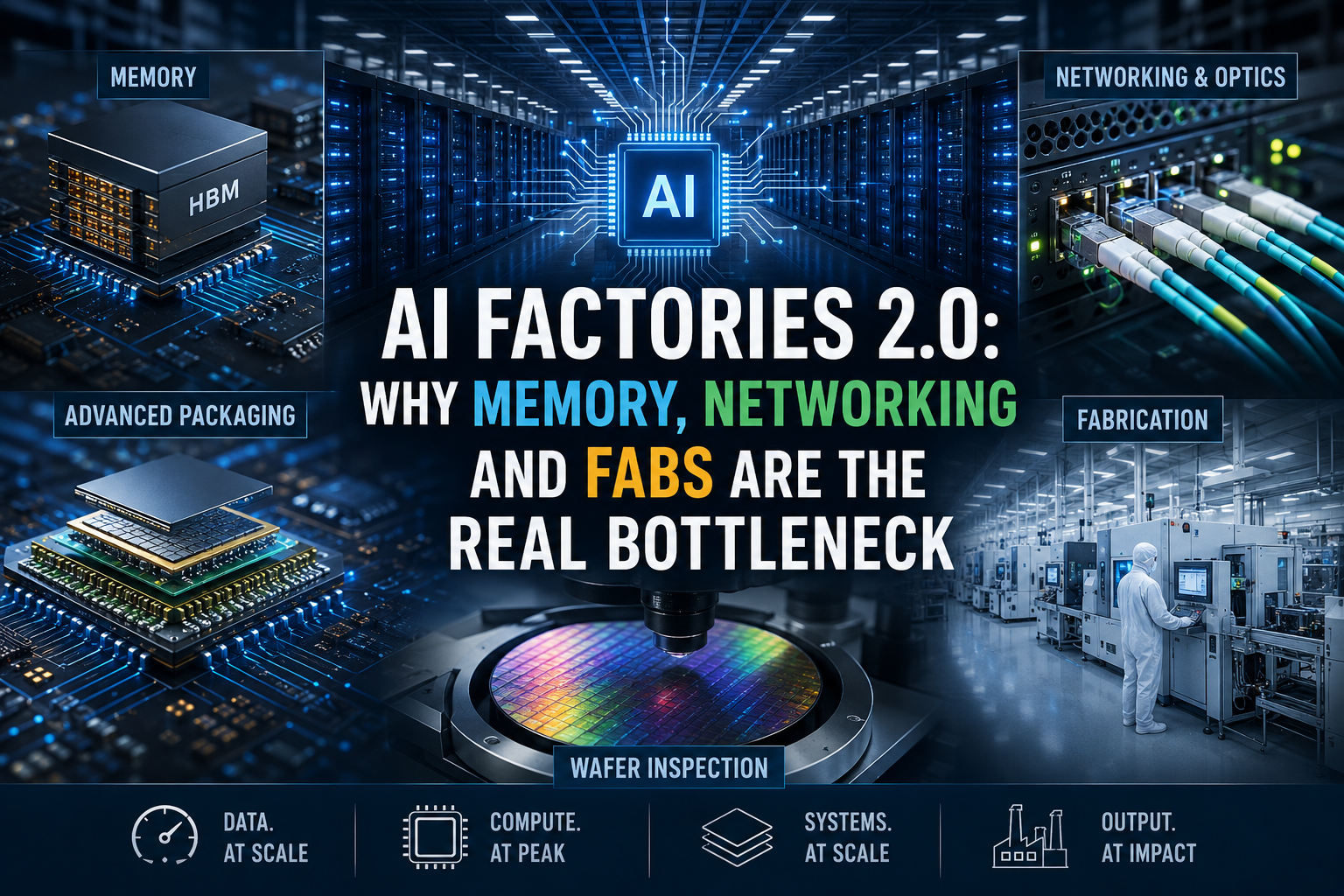
AI Factories 2.0: Why Memory, Networking and Fabs Are the Real Bottleneck
The next era of AI infrastructure will not be won by GPUs alone. Memory, networking, optics, chip packaging, wafer inspection and fab capacity are becoming the real limits of AI scale.
Introduction: The GPU Story Is Too Small
The first wave of generative AI infrastructure had a simple headline: buy more GPUs.
That headline was not wrong. GPUs and AI accelerators are still the visible engines of modern AI. They train models, run inference, power reasoning workloads and turn enormous amounts of data into useful outputs.
But the GPU-only story is now incomplete.
An AI factory is not just a room full of accelerators. It is a production system. Its output is tokens, embeddings, decisions, simulations, recommendations, code and synthetic data. Like any factory, it is limited by the slowest part of the production line.
In AI Factories 2.0, the bottleneck is moving away from raw compute alone. The real constraints are memory bandwidth, high-speed networking, optical interconnects, advanced packaging, semiconductor manufacturing capacity, wafer inspection, yield and factory-scale system design. NVIDIA’s own AI factory materials emphasize high-bandwidth, low-latency networking, orchestration and full infrastructure design, not just accelerator silicon.
The next AI race will not be won only by whoever has the most chips. It will be won by whoever can keep those chips fed, connected, cooled, tested, packaged and productive.
1. The GPU Is the Engine, Not the Whole Factory
A GPU by itself does not create AI output. It needs a full industrial stack around it.
It needs memory close enough and fast enough to feed model weights, activations and key-value cache. It needs a network that can move data between thousands of accelerators without turning synchronization into idle time. It needs advanced packaging that can place compute dies, memory stacks and interposers into one reliable module. It needs wafers, lithography tools, substrates, inspection systems, power delivery, cooling and operational software.
In a small system, the accelerator looks like the center of the world. At factory scale, the accelerator becomes one station in a much larger production line.
That is the key shift from AI Factories 1.0 to AI Factories 2.0.
The old question was: “How many GPUs can we buy?”
The new question is: “How much useful AI output can the whole factory produce per watt, per dollar and per hour?”
2. Memory: The First Invisible Ceiling
Modern AI models do not only need compute. They need memory bandwidth.
During training, accelerators constantly move weights, gradients and activations. During inference, especially with long-context models and reasoning-heavy workloads, memory pressure increases because the system must hold and access more context, more intermediate state and more cached attention data.
This is why high-bandwidth memory, or HBM, has become one of the most important parts of the AI supply chain. HBM is stacked memory placed very close to the AI processor, giving the accelerator faster access to data than traditional memory architectures.
The industry is already pushing aggressively into HBM4. Micron says its HBM4 uses a 2,048-pin interface and delivers more than 2.8 TB/s of bandwidth per stack. Samsung lists HBM4 bandwidth up to 3,300 GB/s and notes that memory performance becomes more important as training and inference requirements converge.
But the deeper issue is not only bandwidth. It is supply, packaging and yield.
Every HBM stack must be manufactured, tested, stacked, connected and integrated with the accelerator package. A shortage of HBM can delay AI systems even when accelerator designs are ready. A yield issue in stacked memory can waste an expensive package. A bandwidth mismatch can leave compute units underused.
In AI Factories 2.0, memory is not a supporting component. It is one of the main production constraints.
3. Networking: When the Cluster Becomes the Computer
As AI systems scale, the network becomes part of the computer.
A single accelerator can run a small workload. A rack can run a larger one. But frontier-scale training and high-volume inference require thousands, tens of thousands or even more accelerators working together. At that point, the network is no longer just plumbing. It is the fabric that determines whether the system behaves like one machine or thousands of isolated chips.
Distributed AI workloads require constant communication. Model parallelism, data parallelism, mixture-of-experts routing, checkpointing and multi-node inference all depend on predictable data movement. If the network has high latency, congestion or jitter, expensive accelerators wait.
That waiting is the hidden tax of AI infrastructure.
NVIDIA describes AI networking as requiring ultra-low latency and high-bandwidth connectivity, with congestion management and adaptive routing used to improve multi-node, multi-GPU performance at scale. Its technical material on Spectrum-X Ethernet Photonics also argues that low-jitter networking is important for reliable token throughput, multi-tenancy and scalable AI factory operation.
The lesson is simple: once the cluster is large enough, networking performance becomes AI performance.
4. Optics: The Cable Is Becoming a Semiconductor Problem
For years, data center networking could scale with copper cables, pluggable optical modules and familiar switch architectures. AI is changing that.
Large AI clusters create enormous east-west traffic, meaning data moves constantly between servers inside the data center. As bandwidth rises, traditional interconnects face pressure from power consumption, signal loss, physical density and reliability.
This is why optical interconnects and co-packaged optics are becoming strategic. Instead of treating optics as a removable module at the edge of the switch, co-packaged optics move optical engines closer to the switch silicon. That can reduce electrical distance, improve bandwidth density and help manage power at very high speeds.
NVIDIA’s Spectrum-X Ethernet Photonics material describes co-packaged silicon photonic engines and optical I/O as part of scaling AI factory networking.
This matters because optics turn networking into a manufacturing problem. Lasers, modulators, fiber attachment, thermal control, test automation and link reliability all become part of the AI factory supply chain.
In other words, the future bottleneck may not be “Can we buy enough GPUs?” It may be “Can we build enough reliable high-speed links to make those GPUs act as one system?”
5. Advanced Packaging: Where Compute and Memory Become One Product
The most powerful AI chips are not simple monolithic chips anymore. They are complex packages made from multiple pieces: compute dies, memory stacks, interposers, substrates and power delivery structures.
Advanced packaging is where the AI accelerator becomes a usable product.
TSMC’s CoWoS technology, for example, is designed for ultra-high-performance computing applications such as AI and supercomputing. TSMC describes CoWoS-S as using wafer-level integration to connect logic chiplets with HBM stacks over a large silicon interposer.
That sounds like packaging, but it is much more than putting a chip in a protective case. Advanced packaging is where electrical distance shrinks, bandwidth rises and memory gets physically close enough to feed the processor.
It is also where the supply chain gets harder.
Large interposers, high-density substrates, micro-bumps, thermal interfaces and stacked memory all introduce manufacturing complexity. The package must deliver performance, power and reliability at the same time. A failure in one component can reduce yield or scrap a very expensive module.
This is why advanced packaging capacity has become a strategic issue. In a 2025 earnings call, TSMC said it was working to double CoWoS capacity that year to support strong customer demand, and it also discussed new advanced packaging facilities as part of its broader AI supply chain expansion.
The takeaway is clear: AI chip supply is not only about wafer starts. It is also about advanced packaging slots.
6. Fabs: The AI Roadmap Is Limited by Manufacturing Reality
AI roadmaps often sound like software roadmaps: faster models, larger clusters, better agents, lower cost per token.
But underneath every AI roadmap is a semiconductor manufacturing roadmap.
Leading-edge AI chips require advanced process nodes, lithography capacity, deposition, etch, metrology, cleanroom space, skilled labor, specialty gases, chemicals, substrates and a long chain of equipment suppliers. These constraints cannot be solved overnight.
ASML describes EUV lithography as using 13.5 nm light to enable high-resolution patterning and mass production of advanced microchips. It also notes that EUV systems are used for the most intricate layers of advanced chips, including leading logic and memory nodes.
That means AI infrastructure is tied to the physical pace of semiconductor manufacturing. New fabs take years to build and ramp. New tools must be installed and qualified. New processes must reach acceptable yield. New packaging lines must scale without breaking reliability.
Software can be copied quickly. Fabs cannot.
This is one of the biggest misunderstandings in AI infrastructure. The demand curve can move like software, but the supply curve still moves like heavy industry.
7. Wafer Inspection and Yield: The Quiet Multiplier
Wafer inspection rarely gets the same attention as GPUs, but it is one of the most important parts of the AI hardware stack.
As chips become larger, denser and more expensive, tiny defects matter more. A particle, pattern defect, overlay issue, bonding problem or substrate flaw can reduce yield. In advanced packaging, the risk multiplies because many components must work together inside one high-value package.
KLA describes defect inspection and review systems as covering yield applications such as wafer qualification, process monitoring, tool monitoring and line monitoring. Its systems inspect patterned and unpatterned wafers, using optical, e-beam and algorithmic methods to find and classify defects.
For AI chips, this becomes even more important because HBM and advanced packaging add more failure points. KLA notes that HBM production requires ensuring each chip in the stack is functional and reliable, because one failed chip can affect the entire HBM component. It also highlights process control for stack assembly and advanced packaging integration.
Yield is not just a manufacturing metric. It is an AI scaling metric.
A better yield means more usable accelerators from the same wafer capacity. Better inspection means faster ramp. Faster ramp means more AI capacity online sooner. In AI Factories 2.0, inspection tools are not background equipment. They are part of the performance supply chain.
8. The New Scorecard for AI Factories 2.0
The next generation of AI infrastructure needs a broader scorecard.
The old scorecard focused on peak compute, GPU count and model size. The new scorecard includes:
Old Metric AI Factories 2.0 Metric
Number of GPUs Useful accelerator utilization
Peak FLOPS Tokens per watt and tokens per dollar
Server count Cluster-level throughput
Network bandwidth Predictable low-latency communication
Chip announcement Manufacturable package volume
Wafer supply Known-good packaged accelerator supply
Model size Memory bandwidth and cache efficiency
Data center size Factory uptime, cooling and power efficiency
This shift changes how AI infrastructure should be planned.
A balanced AI factory is better than a lopsided one. Too much compute without enough memory creates idle silicon. Too much accelerator density without enough network creates congestion. Too much chip design ambition without enough packaging capacity creates delays. Too much fab output without enough inspection and yield control creates waste.
AI scale is now a systems problem.
9. What Builders Should Focus On Next
For companies building AI infrastructure, the lesson is practical: stop treating hardware as a single purchasing decision.
The better approach is to design the AI factory as an end-to-end production system.
That means planning memory capacity and bandwidth early, not after the accelerator decision. It means treating the network fabric as part of the compute architecture. It means understanding optics, switch radix, cabling, failure domains and congestion control. It means tracking advanced packaging capacity and HBM supply as strategic dependencies. It means paying attention to wafer inspection, metrology and yield because these determine how quickly hardware can move from design to deployment.
It also means optimizing for operations.
The best AI factory is not the one with the most impressive peak benchmark. It is the one that stays productive under real workloads, real failures, real power limits and real supply constraints.
Conclusion: The Bottleneck Has Moved to the Factory
AI Factories 2.0 are not just bigger data centers. They are industrial systems built from compute, memory, networking, optics, packaging, fabs, inspection tools, power systems, cooling and software orchestration.
GPUs still matter. But they are no longer the whole story.
The real bottleneck is the full hardware pipeline: memory that can feed the accelerators, networks that can connect them, optics that can scale the fabric, packaging that can integrate compute and HBM, fabs that can manufacture leading-edge silicon, and inspection systems that can protect yield.
The companies that understand this will build better AI factories.
The companies that do not will buy expensive accelerators and wonder why their factory output does not match the promise.
AI is often described as a software revolution. But at scale, it is also a manufacturing revolution.
And in that revolution, the winners will be the ones who master the whole factory.
Tags
#AI #AIFactories #AIInfrastructure #MemorySystems #HighPerformanceNetworking #Semiconductors #ChipManufacturing #AICompute #DataCenters #ScalableAI #EnterpriseAI #AIHardware #DigitalInfrastructure #NextGenComputing #AIEcosystem #TechnologyInnovation #FutureOfAI